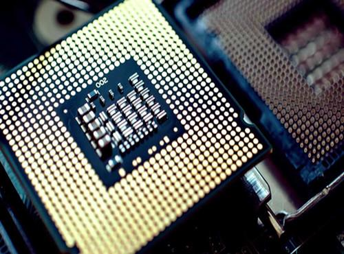
FC-BGA substrates
FC-BGA substrates. ABF series substrates materials. From 5um to 30um gap substrates Manufacturer. FCBGA Flip Chip Ball Grid Array packages from a subgroup of the Flip Chip package family. The FCBGA package is the main platform in this sub-group, which also includes bare die, stiffener only and a thermally enhanced version with one /two piece heat spreader or lid(FCBGA-H), System-in-Package(FCBGA-SIP) versions and a package subsystem meeting the standard BGA footprint that contains multiple components within the same package(FCBGA-MPM).Options also include configurations with thin core, Pb-free and copper column bumps. Flip Chip BGA packages are available in ball counts ranging from 210 to 3000+, board unit sizes from 10*10mm to 55*55mm.
ALCANTA offers a complete FCBGA portfolio for the network, computing and consumer markets, Demand for greater functionality and significantly higher processing speeds in consumer and networking devices is driving flip chip technology to provide cost effective, scalable packages with ultra low K dielectrics, high power integrity , superior thermal performance and higher resistance to electromigration(EM) in very large package sizes, with very fine bump pitches and lead-free solder.
FCBGA package substrate, Flip-chip package substrate, we have made the ball Pitch 160um(6.3mil). laser via drill size 85um. and 25um(1mil) for the laser via copper ring. the pad to pad gap are 12um. Advanced FCBGA package substrate technology. Improve electrical performance and incorporate higher IC functionality: Alcanta Flip Chip BGA (FCBGA) packages are assembled around state‑of‑the‑art, single unit laminate or ceramic substrates. Utilizing multiple high density routing layers, laser drilled blind, buried and stacked vias, and ultra fine line/space metallization, FCBGA substrates have the highest routing density available. By combining flip chip interconnect with ultra advanced substrate technology, FCBGA packages can be electrically tuned for maximum electrical performance. Once the electrical function is defined ,the design flexibility enabled by flip chip also allows for significant options in final package design. Amkor offers FCBGA packaging in a variety of product formats to fit a wide range of end application requirements.
Chip package Substrate Solution: The semiconductor chip industry chain can be divided into three parts: chip deisng, chip manufacturing, and packaging and testing. the semiconductor chip packaging substrate is a key carrier in the packaging and testing process. The packaging substrate provides support, heat dissipation and protection for the chip, and also between the ship and the PCB. Provide power and mechanical connections, Packaging substrates usually have technical characteristics such as thinness, high density, and hgh precision, Alcanta can rpovide chip design companice and packaging and testing companies with Layer Structure Up to 9-n-9 of wire bonding process substrates and flip-chip packaging substrates, These substrates are mainly used for micro-electromechanical systems, radio frequency modules, memory chips,substrates and application processors Package.
About the IC Substrates. FC-BGA substrates. SHDBU substrates. FC-CSP Substrates. CPCORE Substrates. Module Substates. MSD substrates, FR substrates, SEN substrates , MIC substrates design and Fabrication questions. please contact with: info@alcantapcb.com